|
 | Motor Controller Design: A Photo Journal |  | by Ian Hooper, 25th November 2008 | | As many readers will be aware, I've been toying with motor controller design for about 18 months now - working up from very modest (~2kW) designs toward the ultimate goal of a controller suitable for road-going electric cars. You can see details of my first complete controller here: Electric Trolley Speed Controller, or for a more basic introduction to DC motor controllers check out the Tech Info: Controllers section.
In the last few months I've built a few "car-sized" controller prototypes, each time getting a little better, so I thought I'd share a few pictures from the journey.
PS: To anyone who wants full design data, I recommend you start by building something a little more modest, and work your way up! The latest prototype is a pretty tough build. (i.e if the pictures need further explanation, you probably need more experience under your belt first.)
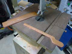
Version 0.1: Seemed like a good idea at the time
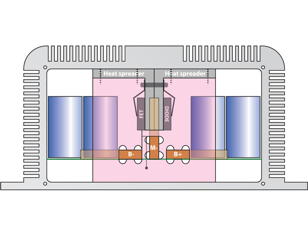
Here was my first attempt at designing the power section for a ~500 amp DC motor controller. In pre-emptive answer to the first question I'm sure people will ask: I'm using IXYS120N20 MOSFETs and STTH6002C diodes - but am definitely open to any other recommendations!
Front view of the proposed power section |
Top view of the proposed power section |
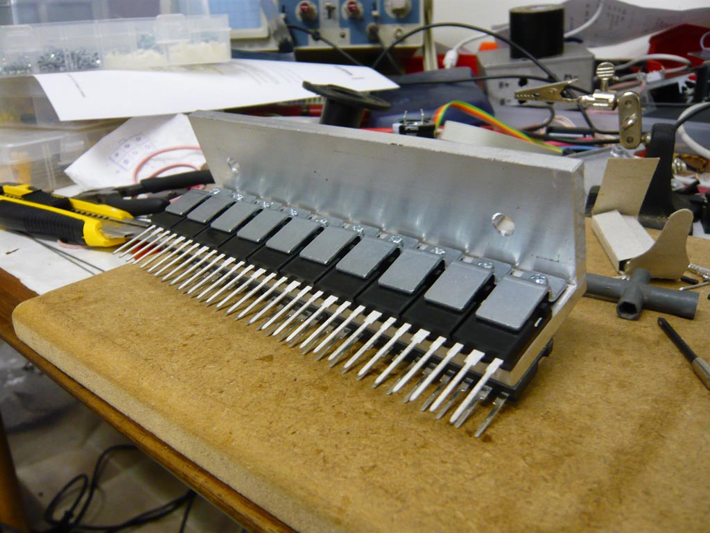
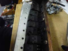
Ten MOSFETs and ten diodes mounted to a heat spreader |
Hmm, how are we going to positively attach those legs to those buss bars? |
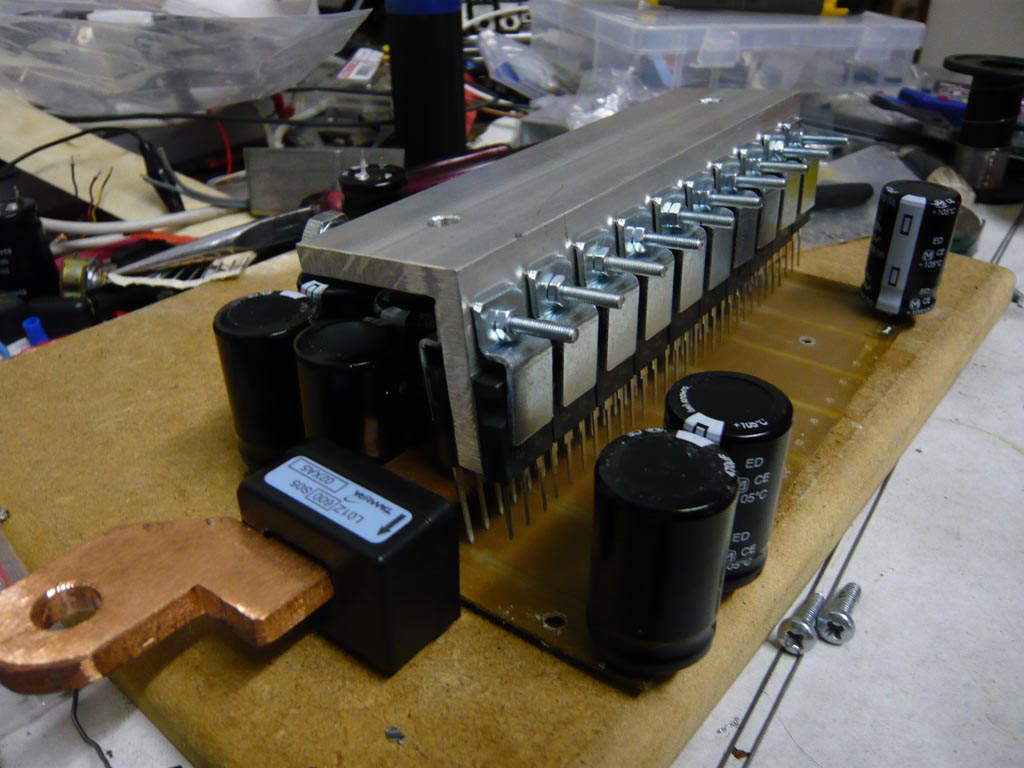
Test fitting the semiconductors on the capacitor board
|
Scabby looking etched PCB for the capacitors |
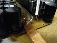
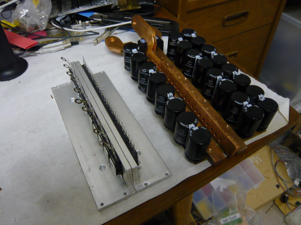
First idea for attaching legs to buss bars: Ring terminals soldered to legs |
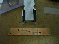
Heat spreader with FETs & diodes on left, capacitor board with buss bars on right |
Scabby looking etched PCB for the capacitors |
I abandoned this design before even completing the power stage because it became apparent how awkward it was using the ring terminals to attach to the buss bars. And tapping that many holes in the copper bars almost drove me mad. (Copper work-hardens so is not fun to tap! In fact the reason for the wire link in the third picture above was due to a tap breaking off in the hole for that strip.)
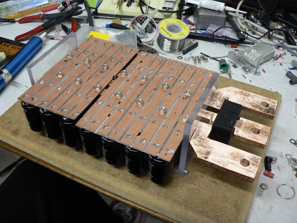
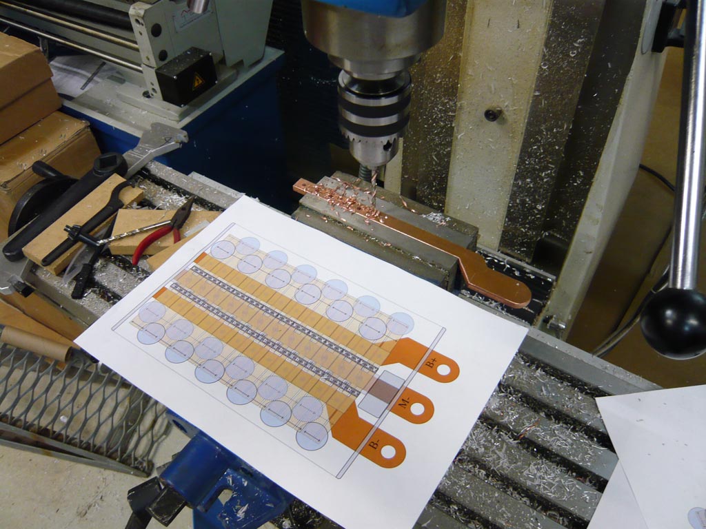
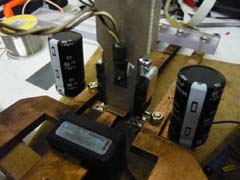
Version 0.2: First one to actually get the MX5 driveable
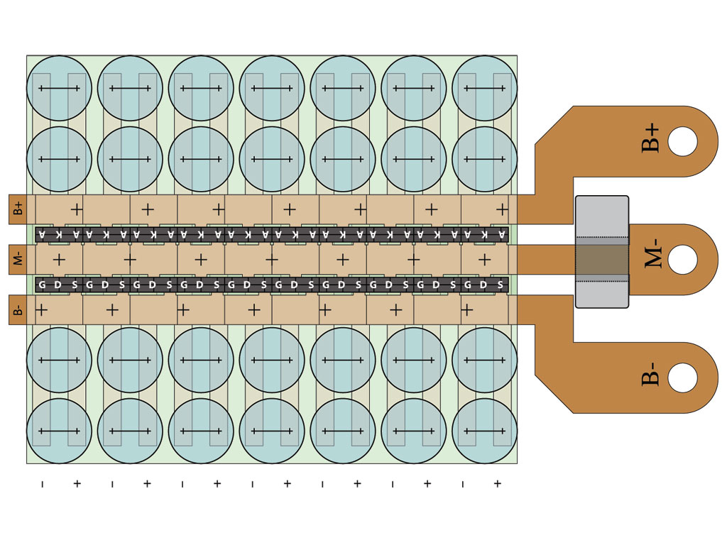
Top view of the updated layout.. All bus bars lying flat, sandwiched between PCB for semiconductors and PCB for capacitors. |
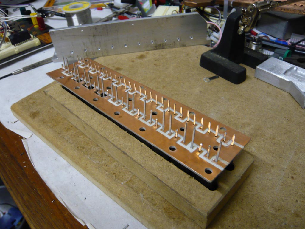
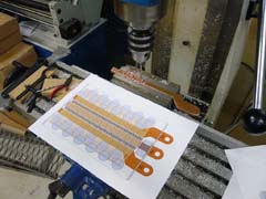
The PCB for the semiconductors has 4oz copper - tough to etch, so I decided to mill it instead. |

Completed PCB board with semis ready to be soldered. (Jig below holding semis to ensure correct height & alignment.) |
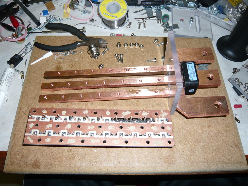
Testing fits with polycarbonate buss bars (its about 10x faster to machine than copper)! |
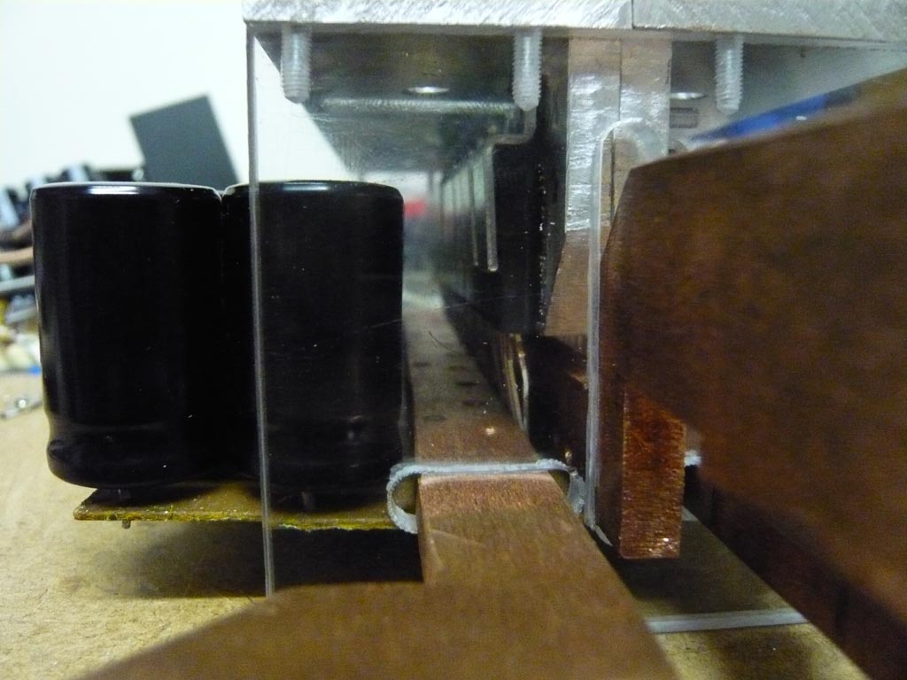
Heat spreader with insulation in foreground, power PCB on fake buss bars in background |
The "real" buss bars. Some (electrically) conductive silver paste on the power PCB before fitting to bars. |
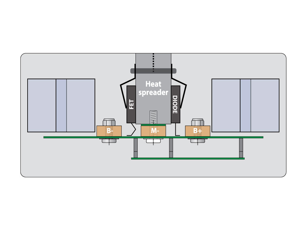
Putting it all together. That's the current sensor mounted on the middle (M-) buss bar, BTW. |

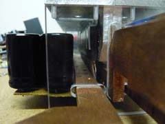
Capacitor boards added, with brass nuts & bolts providing conduction path to buss bars. |
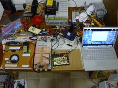
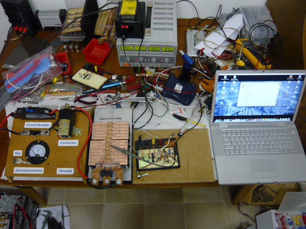
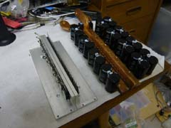
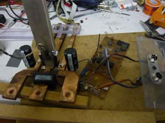
Picture of the (messy) testbench.. Left to right: Test gear, power section, prototype logic board, computer for programming microprocessor. Back left: Older prototypes! |
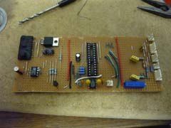
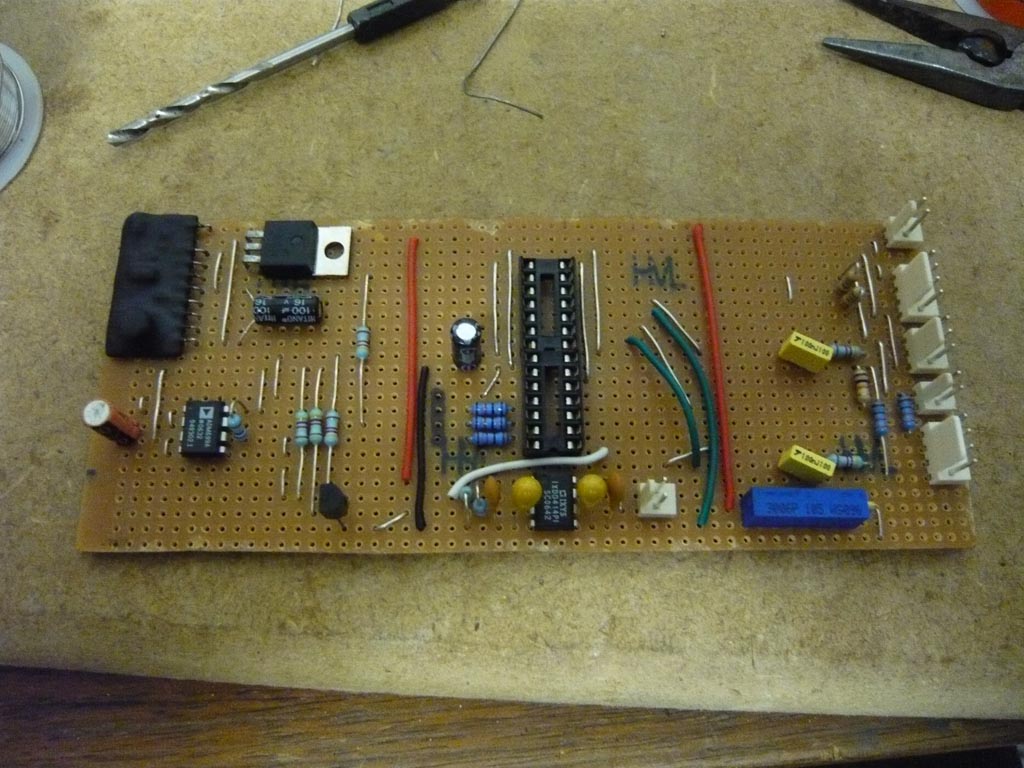
Transferring the logic board prototype to a permanent board. |

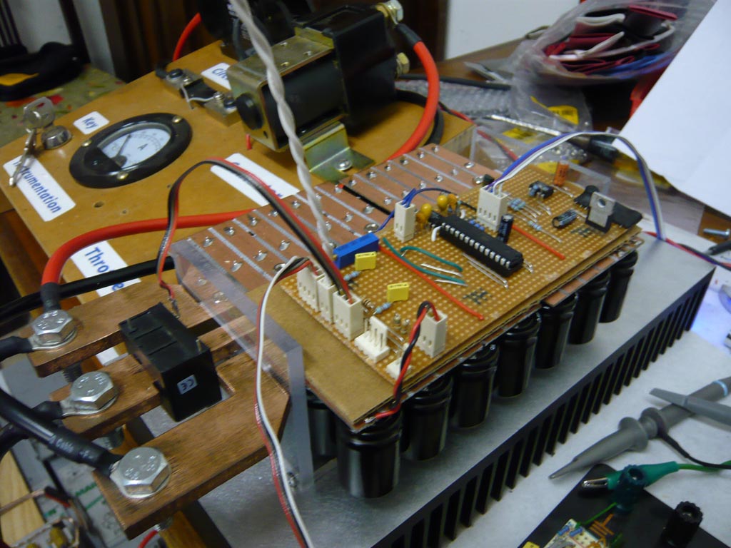
Mounting the logic board beneath the power section. Yes, that's cardboard being used as an insulator :P |

Milling up polycarbonate bits for the case.
(Front panel shown.) |
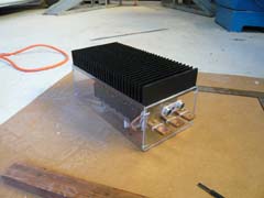
All boxed up and looking pretty. |
Installed in my MX5, still looking pretty. |
Throttle response was surprisingly aggressive... |
Some comments.. Testing was done at 72V, from a bunch of AGMs sitting on the floor, and I've been using an Advanced DC L91 motor as the load (though no actual load on the motor, which seriously restricts the amount of power I can test to). In the car it's a 128V pack running a Warp 11 motor, direct drive to the diff. So polar opposites in terms of load between test bench and vehicle!
To any other budding controller developers out there, I highly recommend you have a circuit breaker in the loop for your testbench. I also found it very useful to test things with only the trickle of current coming through the precharge resistors, since you can be assured nothing particularly bad can happen if something goes wrong!
Of course, field testing is another story..
Version 0.2: Post Mortem!!
Yes, I blew v0.2 up while testing it in the MX5. Let a LOT of smoke out of the MOSFETs. But that's OK.. I'd heard it was inevitable that I'd blow up a whole bank of FETs while developing a controller, so now it's happened - hopefully for the first and last time! Plus, by the time I'd finished building this prototype, I had already thought of a whole lot of improvements to the design.. so it just forced my hand with a rebuild. Anyway, here's some gory pics..
Not looking so pretty anymore, are you!? |
What a mess.. Some tracks on the capacitor board were vapourised. |
A row of black, thoroughly destroyed MOSFETs, many with their legs melted off. |
The reason for this catastrophic failure was actually very simple, a silly coding mistake on my behalf.. *sigh* I had the multiplier for the current sensor out by a factor of two in the software, so it was limiting to 800 motor amps at the time. And the current sensor only works to 750 amps.. so in fact there was no current limiting at all. (And yes, it blew when I was being a little overzealous on the throttle.. but it was very briefly a lot of fun.)
Version 0.3: Back to the drawing board
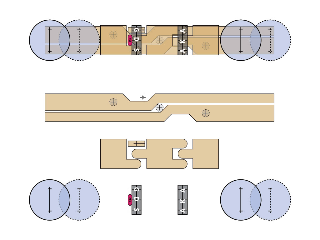
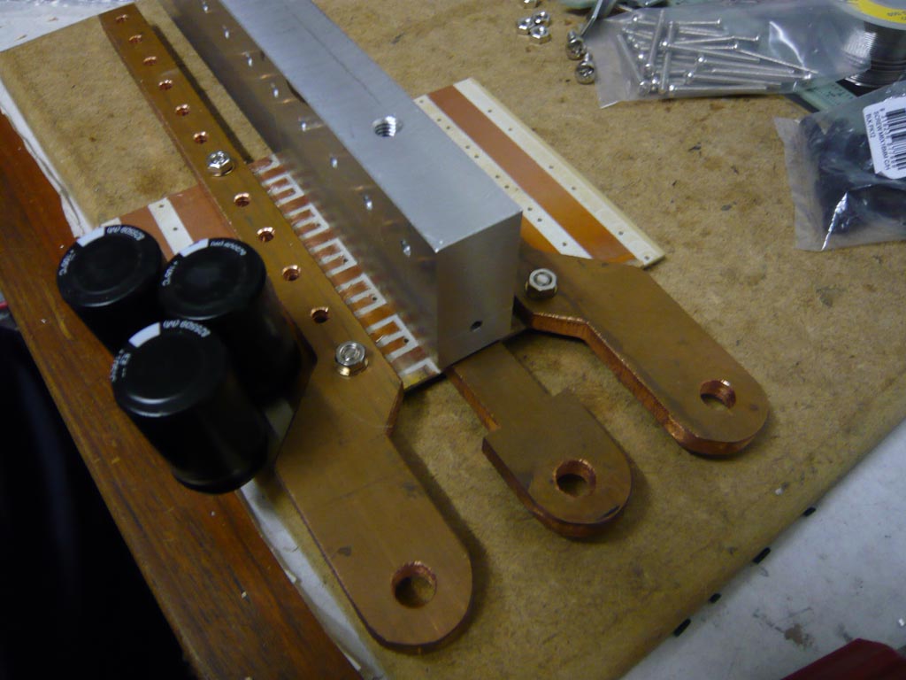
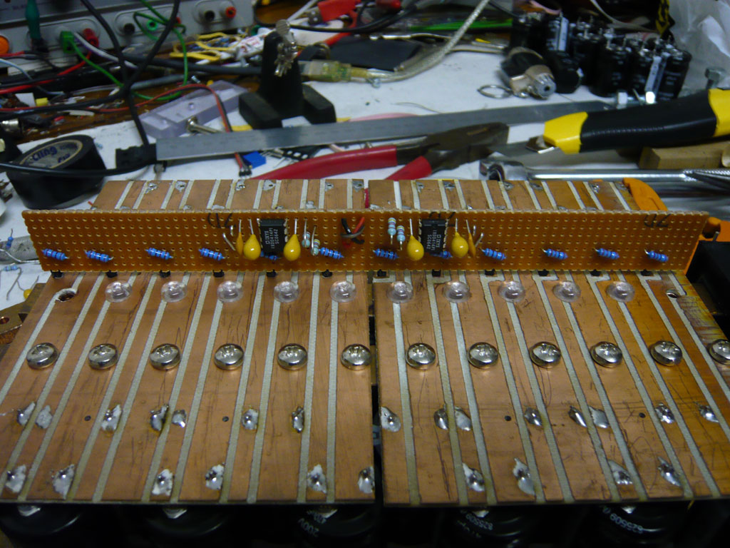
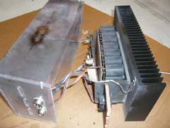
So after blowing ten expensive MOSFETs, it was time to get back to the drawing board. I had a bunch of new improvements in mind, and the destruction of the previous build showed some of the weak links - such as the need for thicker copper on the capacitor board. But this time I started out small-scale, working up from a single FET/diode board of the new design (which I could test right up to the intended 50 amps per pair, even on an unloaded motor) up to a 250A prototype (half scale) to actually test in the car. I also added a motor-side ammeter, both while on the testbench and in the car. (I seriously should have done this much earlier.)
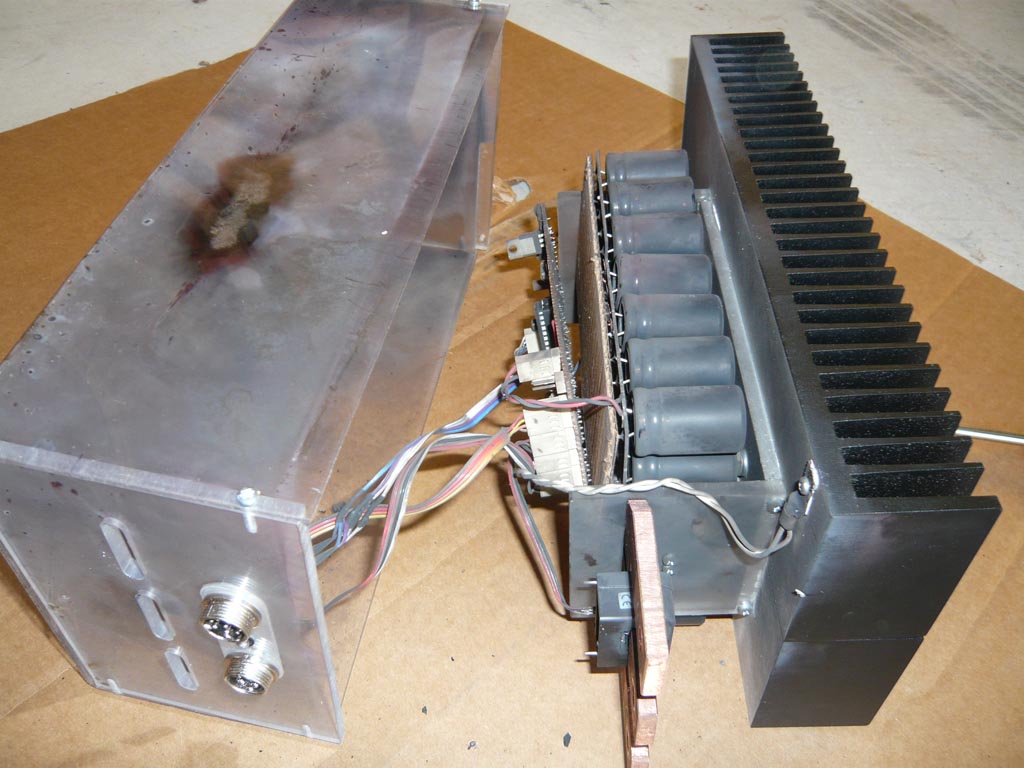
Front view of the updated design. One double-sided PCB with 4oz copper. 20mm heat spreader. Bigger buss bars. Much better. |
Top view and "exploded" view of a single FET/diode/cap board. 15K resistors from gate to ground are also new - a safety measure in case the gate driver fails. |
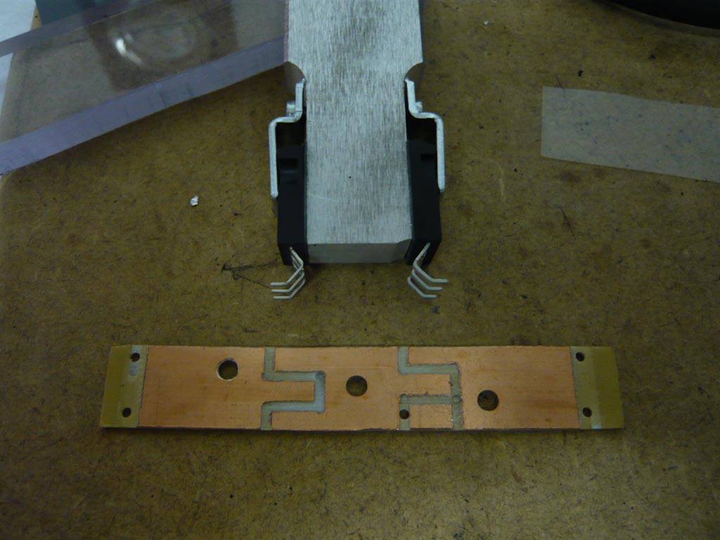
One FET and one diode about to be soldered to a little PCB. The bent legs are to give them some compliance (allowing for thermal expansion, for example). |
Completed "single pair" board including capacitors, mounted to a temporary heatsink. Thermistor visible on the front of that. Using buss bars from v0.2 because I was too lazy to cut new ones :P |
Also too lazy to make a new logic board, but the old one was fine other than a blown FET driver (man I've gone through a lot of those this year!) |
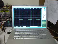
Oscilloscope trace of the output.. looks pretty good if I may say so myself! (Nice sharp edges with fairly small spikes and ringing on the waveform.) |
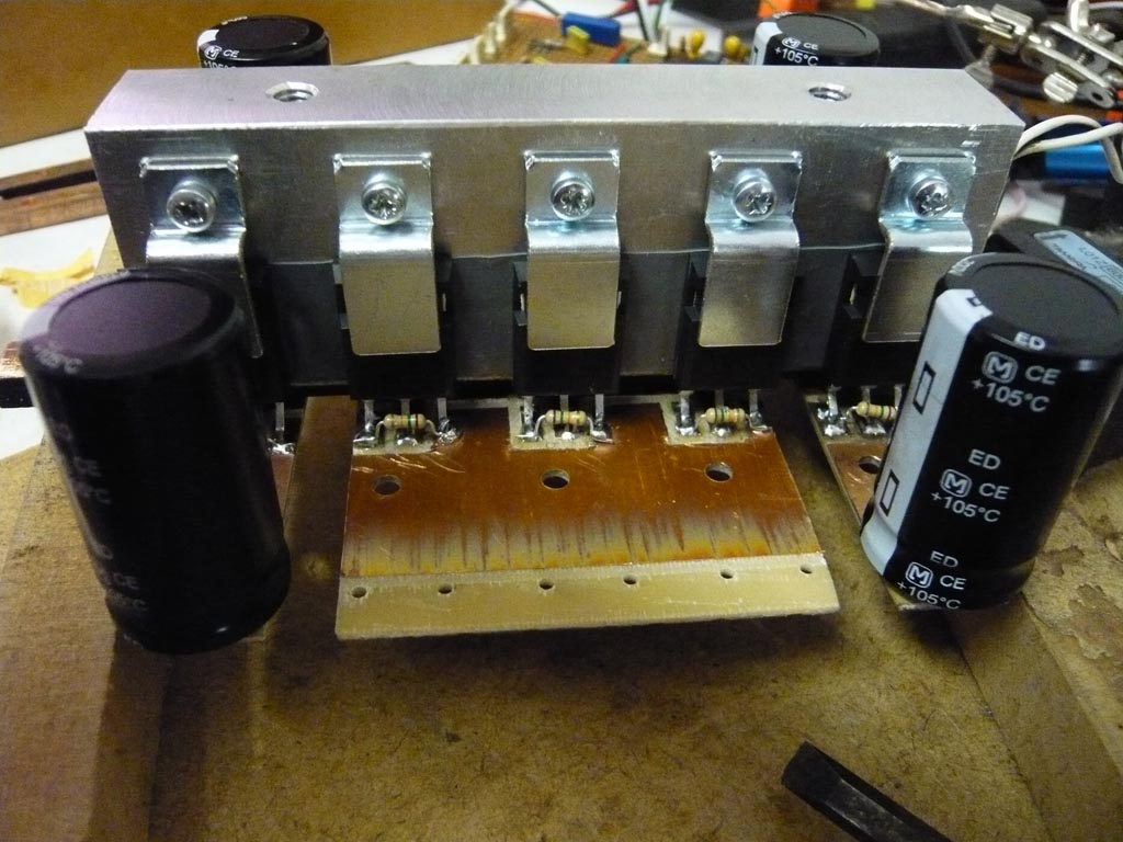
Time to scale things up with another 4 FETs, shown here nearing completion. |

Heatsink mounted to the heat spreader, and some panels being added to hold everything together. Oh and a dodgy gate resistor board. |
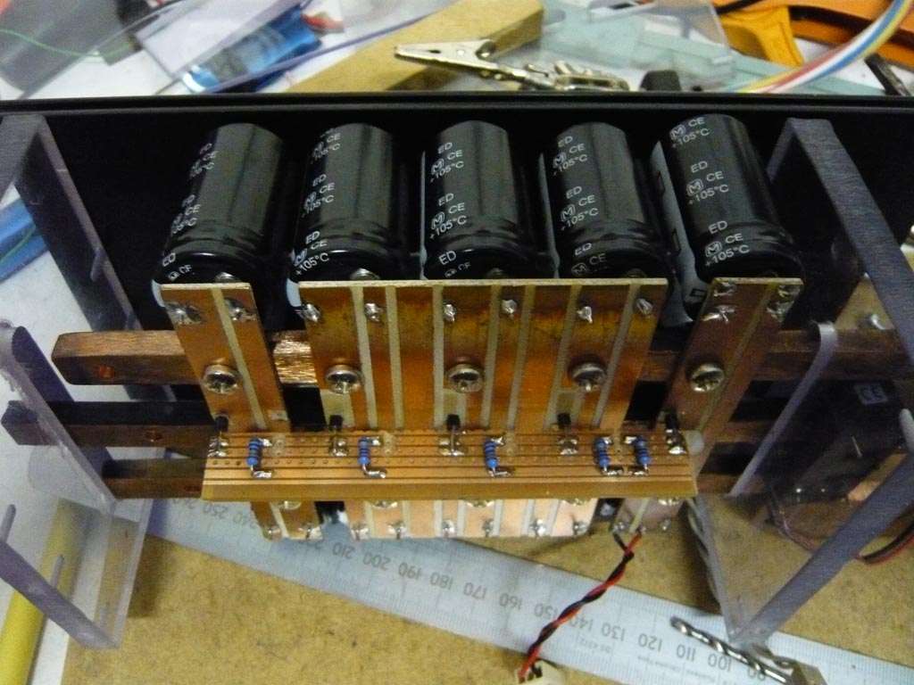
Prototype all assembled including logic board. Since it was only a "half scale" build, I didn't take too much time making this one look tidy. |
After finishing construction, I installed this one in the MX5 for some testing too, and it seemed to work pretty well. Current limit was spot on (I had a motor-side ammeter in the car this time), no smoke came out even when it sat on current limit for a while, and the thermal protection kicked in when it should.
However it became very apparent that 250 amps is nowhere near enough to move a car around, especially when driving a Warp 11 in a direct drive conversion! The Warp 11 dyno chart shows torque about 80Nm at 250 amps (~100kg force at wheels) and 220Nm at 500 amps (~300kg force at wheels, or ~0.3G acceleration). Based on what 80Nm felt like, I didn't think even 220 would be much fun! So while the design seemed to work well, I decided I'd better shoot for a bit more than 500 amps with the next build.
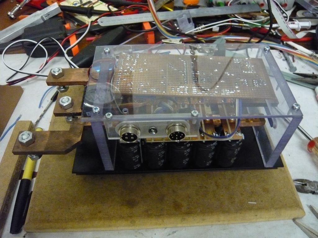
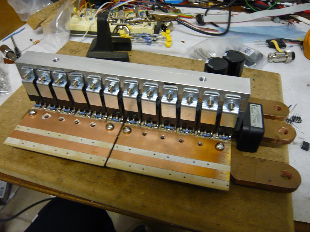
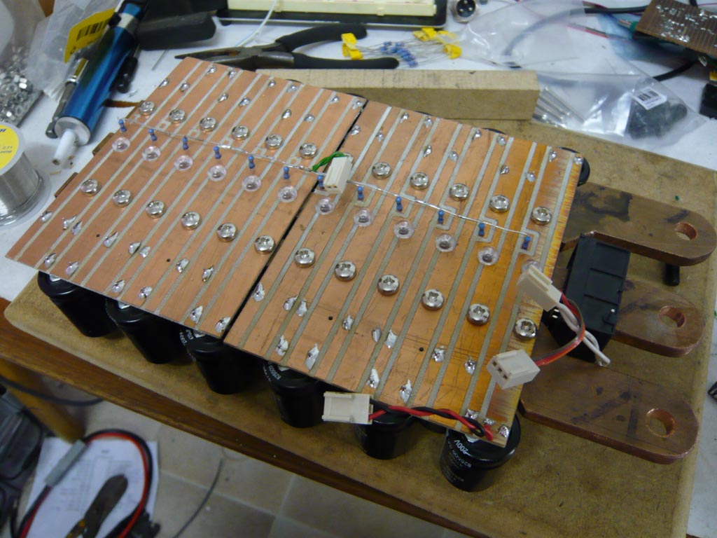
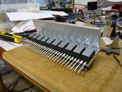
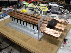
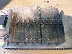
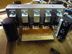
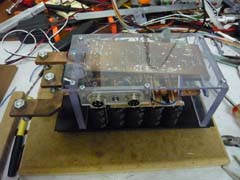
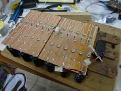
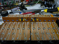
Version 0.4: A 600 amp build of the latest design
This build was much the same as v0.3, other than using 12 pairs of FETs/diodes (600A limit) instead of 5 (250A limit) - and with a smaller spacing between them.
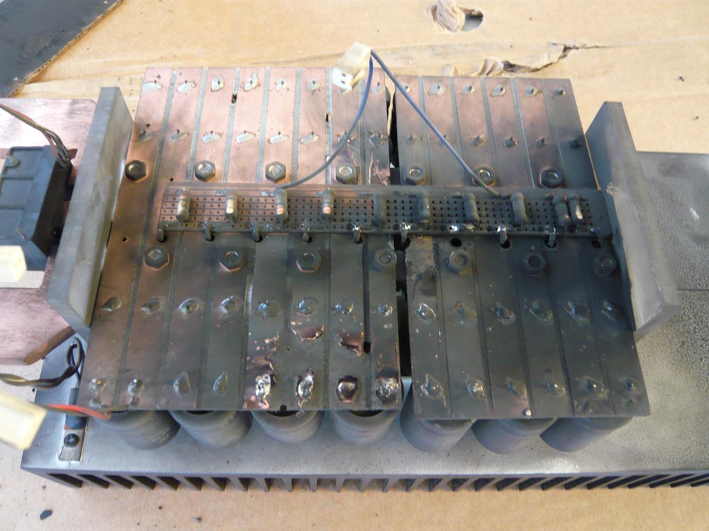
Top view of the 600A power section.
Pretty tidy I think. |
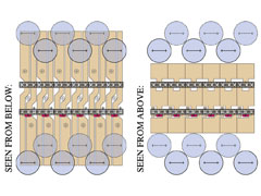
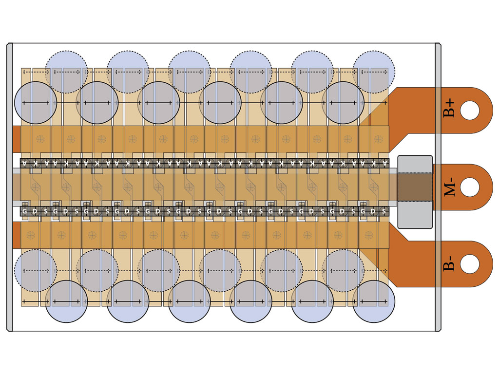
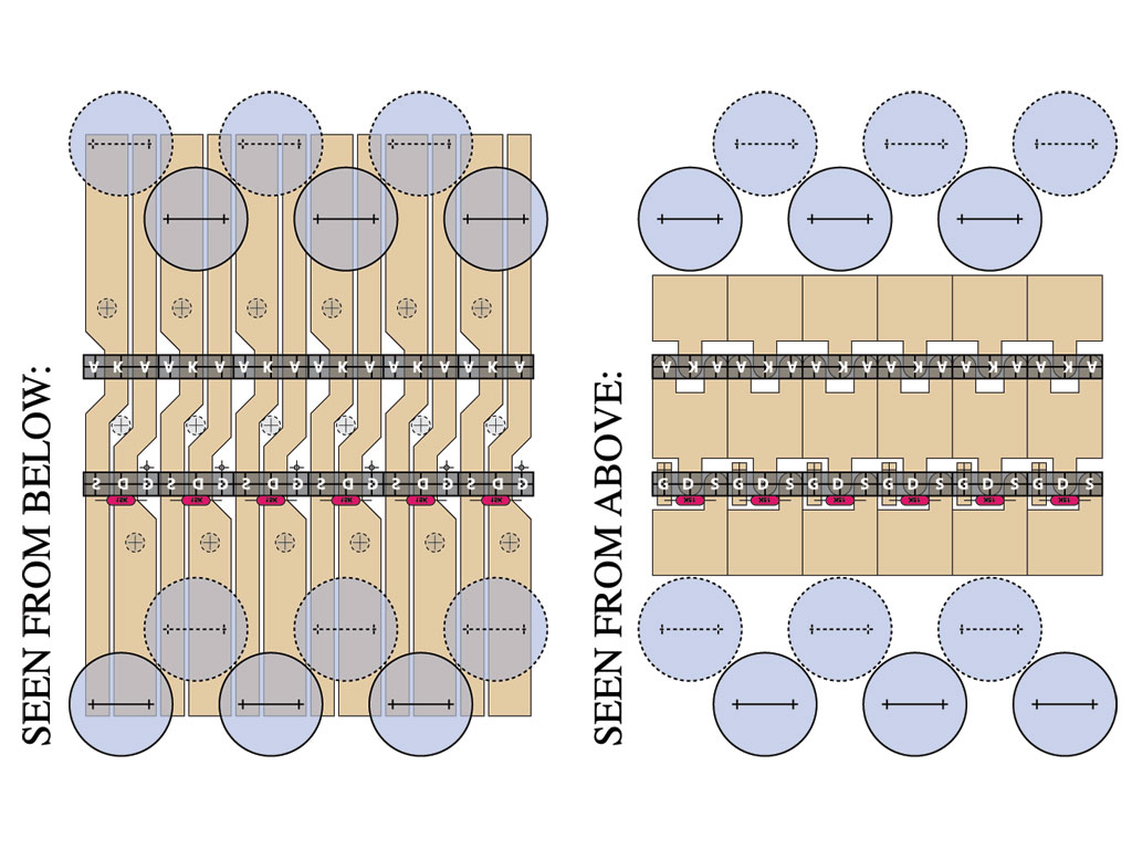
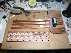
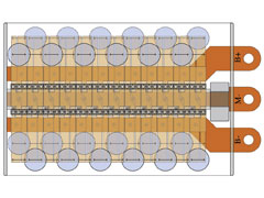
I ended up making two boards of 6 pairs. Here's the top and bottom views of the PCB. |
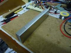
The heat spreader, a 200x40x20mm aluminium block with a bunch of holes. |
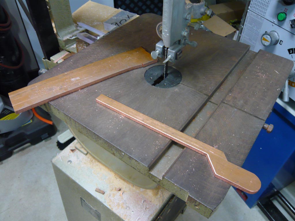
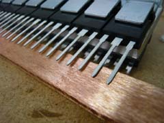
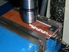
Cutting out new buss bars. I really should shell out for a better bandsaw, this one is painfully slow cutting copper. |
Drilling holes into the buss bar. My mill has a DRO which is invaluable for doing things accurately! |

Test fitting the buss bars to one of the PCBs (here's one I prepared earlier..?) and heat spreader. |
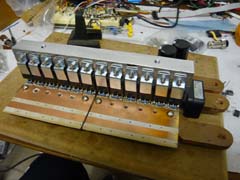
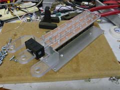
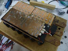
Both boards installed with all the semis attached. |
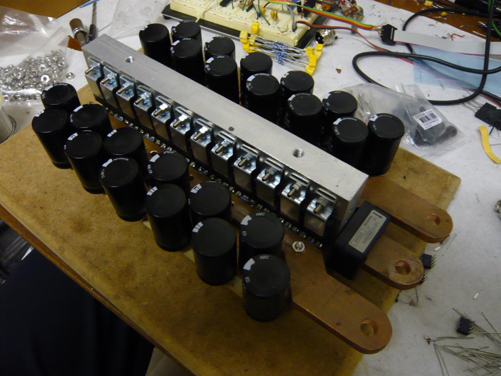
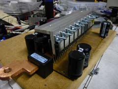
With all the capacitors added. |
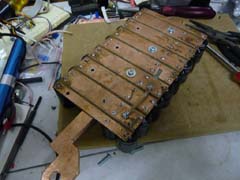
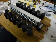
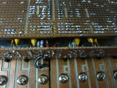
Bottom view, all the bolts holding buss bars to PCB and (nylon bolts) through to spreader. And some of the logic/sensor wiring in place. |
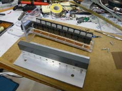
Logic board in place, with fibreglass insulator between it and power board. |
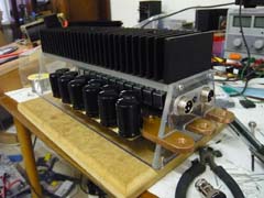
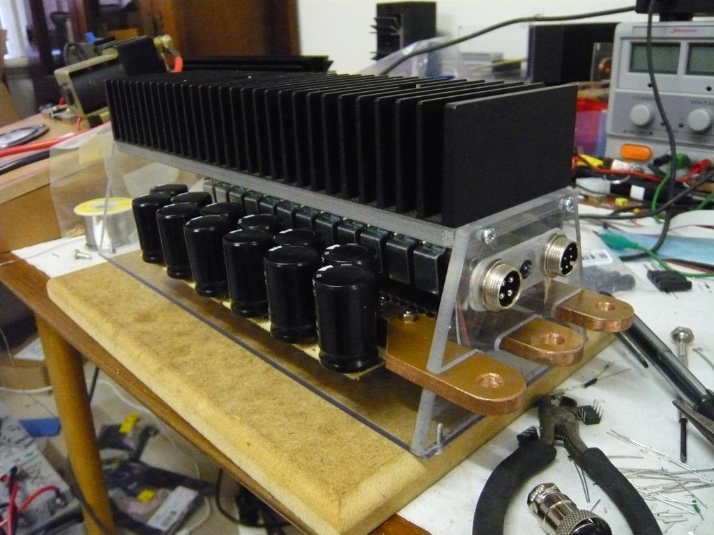
Heatsink bolted to heat spreader and some crude polycarbonate panelling to hold everything together.
|
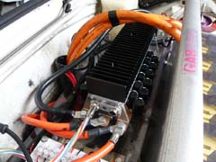
Installed for testing in the MX5. |
Version 0.5 and beyond.. (Or, what's next?)
The latest build seems to function well, except it overheats quickly if it's doing much work.. Much worse than I was hoping, considering (on paper) it has lower on-resistance through the FETs and lower voltage drop through the diodes than a Curtis 1231C! So what might be the problem?
- Switching losses:
MOSFETs don't waste much power when fully on (or off) but during the transition they have a huge voltage drop. I'm using 30 ohm gate resistors, lower value resistors would speed up switching time. Theoretically the IXDD414 driver chip can pump out 14A max so would be OK with gate resistors down to about 10 ohm (might be pushing my luck, but 20 ohm wouldn't be unreasonable). Of course the other problem with faster turn-on/off is the increase in voltage spikes etc. Anyway, I'll have to get an oscilloscope onto the gates to check switching time and do some calculations for switching losses, to see how significant it is.
- Synchronous Rectification:
This is an effective technique for improving efficiency (i.e reducing heat buildup) by replacing the high-side diodes with MOSFETs. Diodes have a steady state voltage drop, so power loss goes up linearly with current (slight simplification), whereas MOSFETs have an on-resistance so power loss increases with the square of the current - but are actually much lower than the diode for typical current levels. The crossover point for the devices I'm using is about 60 amps, so for all but full power synchronous rectification should be significantly more efficient.
Of course, unlike the passive diodes, MOSFETs need to be deliberately turned on and off, and this has to be done with a floating gate supply (grounded to M-).. And there is the issue of dead time, where you need to turn one MOSFET off fractionally before the next turns on to avoid shoot-through... Arr more things to learn! (And most likely, more components to smoke through experimentation!)
- Something else entirely? You tell me ;)
Of course it has been rightly suggested that I could just add better cooling (fan forced convection or water cooling) but that seems like treating the symptom not the cause!
3 December 2008: Minor update
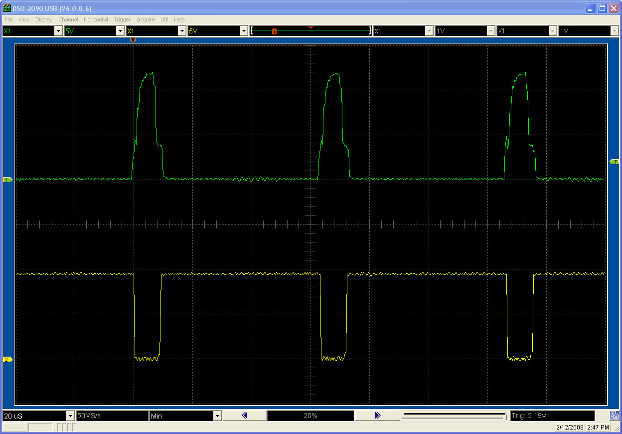
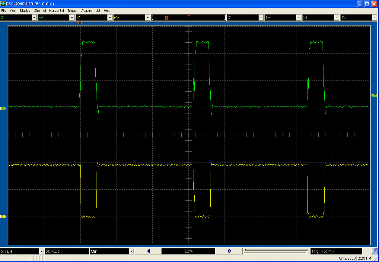
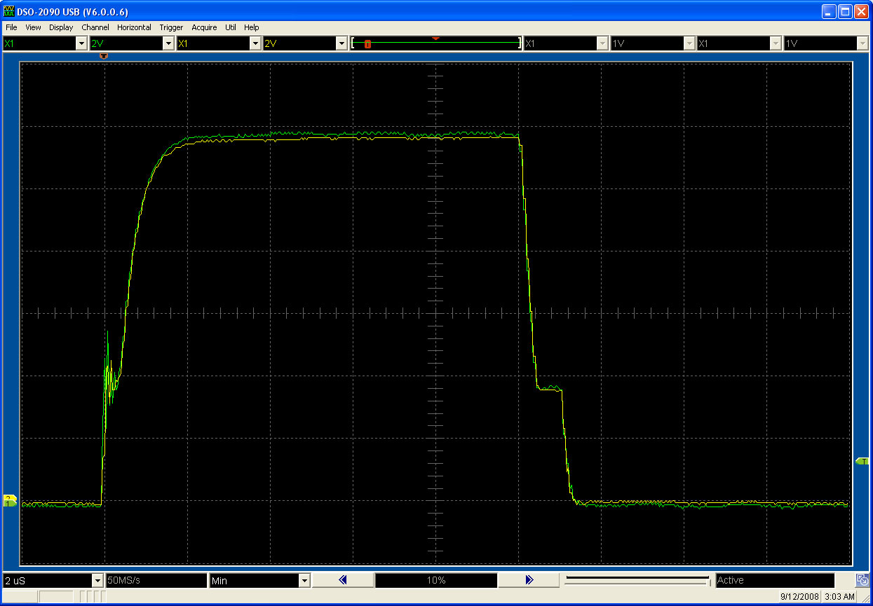
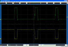
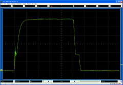
As mentioned above, a good place to start diagnosing the apparently low efficiency of the controller is to get some oscilloscope probes onto the FETs to observe the switching waveforms. So, here they are.
- The GREEN trace is the gate on one of the MOSFETs (presumably they're all pretty much the same?!)
- The YELLOW trace is M- to B-, i.e Drain to Source on the MOSFETs, with the probe set to 10x (so multiply voltage scale by 10.. testing on a 96V nominal bank of AGMs, for reference).
The top image shows a few cycles, frequency is 16kHz. The bottom waveform is the same PWM duty but showing a closeup of a single "on" time. (By the way, the 4-5 pixel noise on all plots is actually due to my cheap and nasty USB scope, and it remains even when the probes are grounded - so is not a fault of the controller! Just ignore it.)
Certainly looks like we could do with faster switching. So next step will be testing lower value gate resistors, and probably divide the load across multiple FET drivers. |
|
8 December 2008 Update: Faster Switching
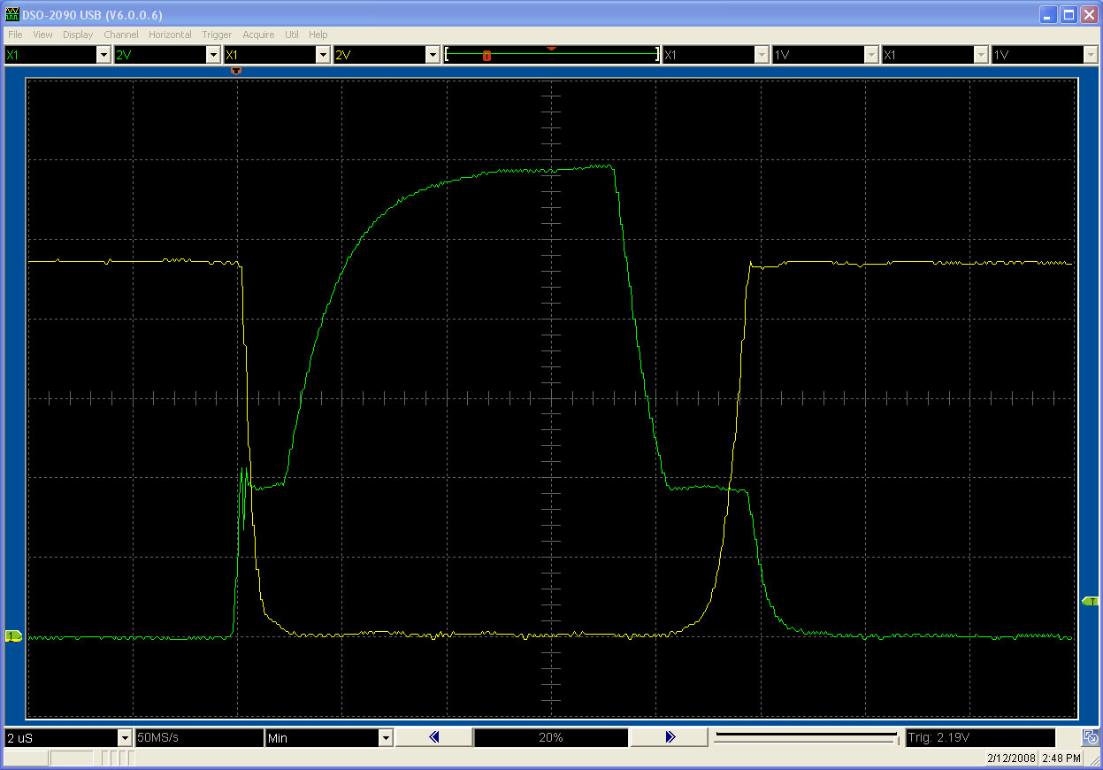
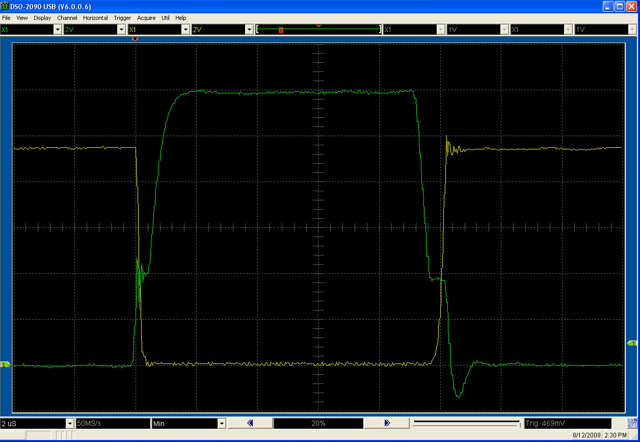
After some helpful discussion and advice from the experts on the EVTech mailing list (thanks guy!) I went ahead with trying to speed up switching times. I built a new "sub-board" with two gate driver ICs instead of one (so they only have to run 6 FETs each, which is easier on the drivers and allows for shorter distances to gates). Gate resistors are now 10 ohm instead of 30 ohm, so turn on/off times should be 3x faster!
Once again there are some screen captures from the oscilloscope, with the same scale(s) as before for comparison. Again, green is the FET Gate and yellow the Source (i.e M-), both referenced to ground.
As you can see with the faster switching, we're starting to see some ringing and overshoot on the waveforms, which would only get worse with even faster switching. So this may be approaching the practical limits of the current design. Of course, it may be possible to get cleaner and faster swiching with a superior electrical design and/or physical layout e.g shorter tracks to gates, more FET drivers distributed along the board, etc.. Let me know if you have any other ideas! (It's gotta be better than a 1231C now though, surely..?)
The new "driver board" beneath the FETs. Ultimately this would all be integrated on the logic board. |
Running at about 15% throttle, axes scaled to show a few PWM cycles |
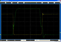
A close-up of one cycle, still at about 15% throttle (i.e we're seeing much less than one period) |
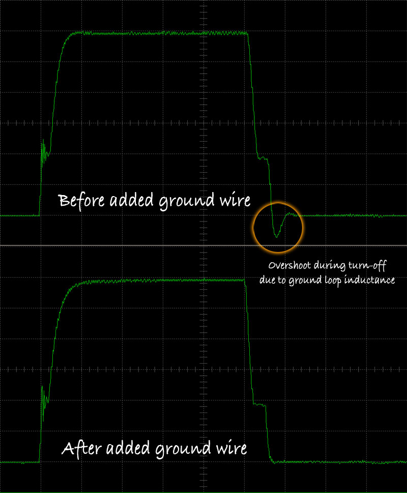
Another significant improvement was the addition of a ground wire between the middle of the driver board and the closest point on the power board, which minimises the group loop trace length (and hence inductance).. Simply eliminated the overshoot observed during turn-off. Amazing what a difference track lengths can make!
Short grounding wire added between logic board ground and B- on the power board. |
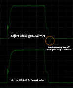
Clear improvement observed in the
gate waveform during turn-off |
Comparing closest and farthest FET gates from the driver to confirm synchronisation - looks good. |
Anyway, I'll get the controller into the MX5 tomorrow and see how it goes - hopefully there'll be a significant improvement.
May 2009 Update: What's been happening?
Well, due to other distractions, not a lot of further development has been happening with the motor controller! The only functional change since December is that it's now running four FET drivers instead of two (so, driving three FETs each) through 5 ohm resistors, which further reduces switching losses. Unfortunately it was still overheating pretty quickly in the MX5.
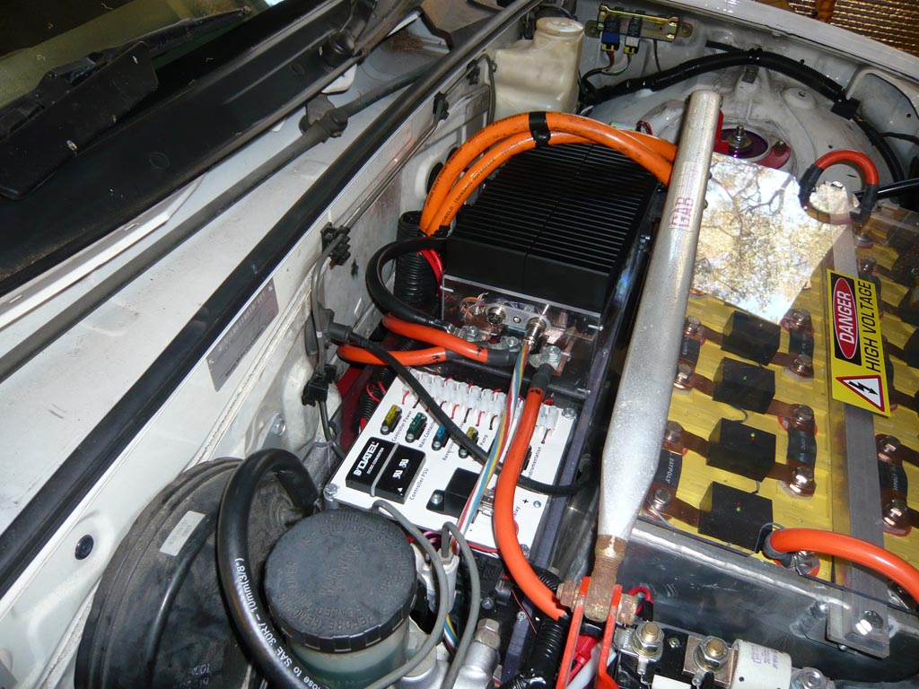
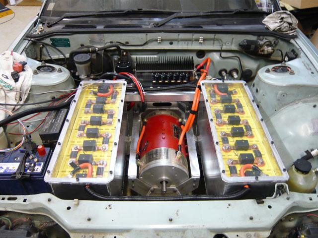
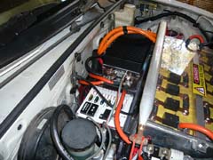
For the last month or two the prototype has been installed in a Nissan Silvia conversion (engine bay pictured right). I had to add forced convection cooling in the form of two 5" computer fans blowing down onto the heatsink, and this pretty much eliminated overheating issues. The controller has been running without fault since, including some pretty tough duty (e.g hillclimbing at 500A continuous). |
|
Of course, in my opinion extra cooling is still just a workaround for inefficiency, so I'm still hoping to experiment with Synchronous Rectification in future motor controller builds. I'll also switch to the impressive new IRFP4668 MOSFET which offers much lower on-resistance than the IXFK120N20s I have been using, which should further help with efficiency.
|